
Japan Semiconductor Materials Market Outlook 2021-2031F
Market Size, Share, Trends, Opportunities, and Competitive Analysis - Segmented by Material Type (Silicon Wafers, Photoresists and Process Chemicals, and Other Materials); Process Stage (Front-End Wafer Fabrication, Lithography, and Back-End Packaging); Technology Node (Mature Nodes, Leading-Edge Nodes, and Advanced Packaging); and Region
Japan Semiconductor Materials Market to Reach USD 20.2 Billion by 2031, Growing at a 7% CAGR: How Wafer and Photoresist Leadership, Rapidus and Advanced Packaging Are Shaping Demand

Japan Semiconductor Materials Market Overview
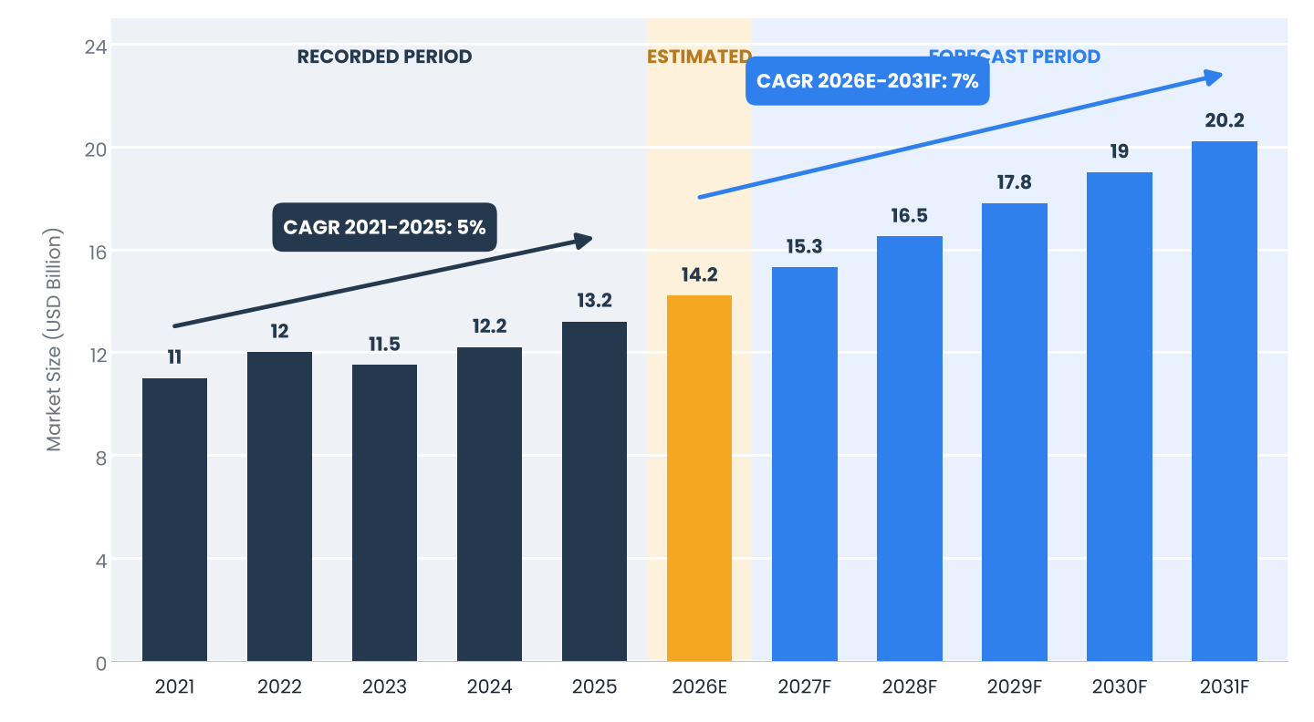
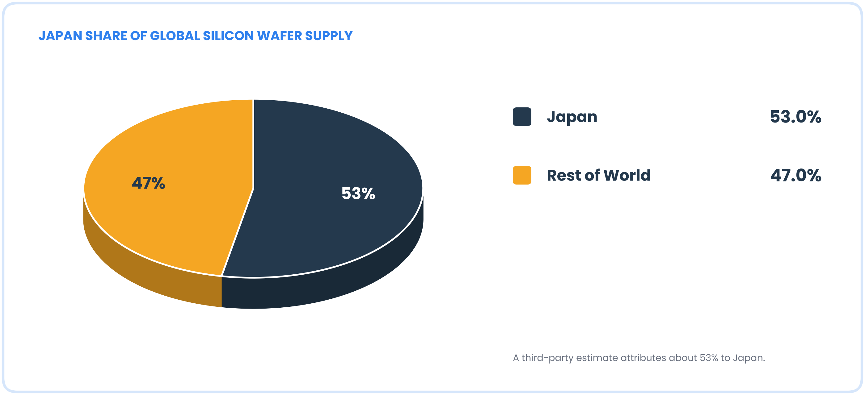
Japan holds a central position in the semiconductor supply chain through the materials that chipmakers depend on. Neargoal Consulting estimates the market at about USD 13.2 billion in 2025, rising to USD 14.2 billion in 2026E and USD 20.2 billion by 2031, a 7% CAGR over 2026E-2031F, after a 5% CAGR over 2021-2025. A third-party estimate attributes about 53% of global silicon wafers and about 50% of global photoresists to Japan.
Key Takeaway Japan's strength is concentrated in a few critical materials. Suppliers that extend leadership from wafers and photoresists into advanced packaging and leading-edge process chemicals will capture growth, while demand cycles and export controls remain the main risks. |
Table 1: Japan Semiconductor Materials Market: Key Insights
Metric | Finding |
Market Definition | Value of Semiconductor Materials Sales by Suppliers in Japan, Including Wafers, Photoresists and Process Chemicals (USD Billion) |
Base Year / Estimated Year | 2025 / 2026E |
Forecast Period | 2027F-2031F |
Market Size, 2025 | USD 13.2 Billion |
Market Size, 2026E | USD 14.2 Billion |
Market Size, 2031F | USD 20.2 Billion |
Recorded CAGR, 2021-2025 | 5% |
Forecast CAGR, 2026E-2031F | 7% |
Japan Share of Global Silicon Wafers | About 53% |
Japan Share of Global Photoresists | About 50% |
Rapidus Government Funding | More Than USD 6.1 Billion |
Rapidus 2 nm Mass Production Plan | 2027 |
Leading Material Type | Silicon Wafers |
Fastest-Growing Segment | Advanced Packaging Materials |
Key Constraints | Export Control Exposure, Demand Cyclicality and Labor Shortages |
Source: Neargoal Consulting Analysis | |
Market Outlook
Our study estimates the market will grow at a 7% forecast CAGR (2026E-2031F) from USD 14.2 billion in 2026E, after a 5% CAGR over 2021-2025. The base case assumes demand follows semiconductor investment in Japan and overseas, that leading-edge and advanced packaging materials grow faster than mature-node materials, and that Rapidus and new fabrication capacity add domestic demand from 2027F.
Figure 1: Japan Semiconductor Materials Market Size, 2021-2031F (USD Billion)
Source: Neargoal Consulting Analysis
Market Dynamics
Growth Drivers
- Global Leadership in Critical Materials. A third-party estimate attributes about 53% of global silicon wafers and about 50% of global photoresists to Japanese suppliers.
- Government Support. Japan has provided about USD 25.7 billion, or 0.71% of GDP, to its semiconductor industry over three years, according to an April 2024 report, including more than USD 6.1 billion to Rapidus.
- New Domestic Fabrication. Rapidus plans mass production of 2 nm chips in 2027, and TSMC is building two plants in Kumamoto Prefecture, which raises local demand for materials.
Restraints
- Demand Cyclicality. Materials demand follows chip production, which swings with end-market cycles.
- Export Control and Geopolitical Exposure. Sales to China and supply chain rules can change quickly.
- Labor and Capacity Constraints. Skilled labor and cleanroom capacity limit expansion pace.
Opportunities
- Advanced Packaging Materials. Substrates, resins and films for chiplet and three-dimensional packaging.
- Leading-Edge Photoresists and EUV Materials. Materials for the most advanced lithography.
- Domestic Fab Supply. Local supply to Rapidus and new Japanese fabrication plants.
- Large-Diameter and Power Wafers. Wafers for power and automotive chips.
Policy and Regulatory Landscape
Japan supports semiconductors through subsidies for domestic fabrication, research funding and public investment in Rapidus, coordinated by the Ministry of Economy, Trade and Industry. Export control rules govern sales of sensitive materials and equipment, and allied-country coordination affects shipments to some markets. The full report assesses how subsidies, export controls and trade policy affect supplier strategy.
Segment Insights
The full report quantifies every segment; the highlights below cover Material Type, Process Stage, and Technology Node.
By Material Type
Silicon wafers take the largest share, while photoresists and process chemicals are critical for lithography.
By Process Stage
Front-end wafer fabrication takes the largest share of materials spending, covering wafers, gases and chemicals. Lithography materials, led by photoresists, are smaller but critical and highly concentrated. Back-end packaging materials grow fastest as advanced packaging expands. Our analysis expects back-end materials to gain share through 2031F.
By Technology Node
- Mature Nodes. Large volumes for automotive, industrial and power devices.
- Leading-Edge Nodes. Higher-value materials for advanced logic, including 2 nm production plans.
- Advanced Packaging. Materials for chiplets and stacked packages.
Geographic Insights
Production and demand cluster around established materials regions and new fabrication sites.
Figure 2: Japan Share of Global Silicon Wafer Supply
Source: Neargoal Consulting Analysis
- Kanto. Headquarters and research for major materials suppliers.
- Kansai and Chubu. Chemical and wafer production bases.
- Kyushu. A semiconductor cluster including TSMC plants in Kumamoto.
- Hokkaido. Home to the Rapidus fabrication site at Chitose.
Competitive Landscape
Key participants include Shin-Etsu Chemical, SUMCO, JSR, Tokyo Ohka Kogyo, Resonac, Fujifilm, Sumitomo Chemical and Rapidus as a customer. Competition rests on technology leadership, purity, qualification with chipmakers and long-term supply relationships. A few suppliers dominate wafers and photoresists.
Shin-Etsu Chemical | SUMCO | JSR | Tokyo Ohka Kogyo |
Resonac | Fujifilm | Sumitomo Chemical | Rapidus |
Key Developments, 2022-2027
- 2022. The government founds Rapidus, which has received more than USD 6.1 billion in public funding.
- April 2024. A report finds Japan has provided USD 25.7 billion, or 0.71% of GDP, to its semiconductor industry over three years.
- 2025. Japan's semiconductor market is estimated at USD 51.9 billion by a third-party tracker.
- 2027. Rapidus plans mass production of 2 nm chips.
What This Means for Decision-Makers
- Materials Suppliers: Extend leadership into advanced packaging and leading-edge chemistries.
- Chipmakers: Secure long-term supply and qualify second sources where possible.
- Policymakers: Pair subsidies with workforce and supply chain resilience.
- Investors: Track capital spending by chipmakers and node mix.
About the Report
Table 2: Japan Semiconductor Materials Market: Report Coverage
Coverage Area | What the Report Covers |
Market Size and Forecast | Revenue (USD Billion) and Volume Views, 2021-2031F |
Segmentation | Material Type, Process Stage and Technology Node |
Geography | Kanto, Kansai and Chubu, Kyushu and Hokkaido |
Competition | Suppliers, Qualification and Share Tracking |
Policy and Constraints | Subsidies, Export Controls and Cyclicality |
Outlook and Recommendations | Supplier Strategy and Guidance by Stakeholder |
Source: Neargoal Consulting Analysis | |
The research report, Japan Semiconductor Materials Market Outlook 2021-2031F - Market Size, Share, Trends, Opportunities, and Competitive Analysis - Segmented by Material Type (Silicon Wafers, Photoresists and Process Chemicals, and Other Materials); Process Stage (Front-End Wafer Fabrication, Lithography, and Back-End Packaging); Technology Node (Mature Nodes, Leading-Edge Nodes, and Advanced Packaging); and Region, covers sales of semiconductor materials by suppliers in Japan, including wafers, photoresists and process chemicals, with a 2025 base year, a 2026E estimate and a 2027F-2031F forecast. It excludes semiconductor equipment and finished chips. Market estimates and projections are based on Neargoal Consulting’s proprietary research methodology, exhaustive primary and secondary research.
For questions about report coverage, methodology, suitability, etc.
For requirements beyond the published report